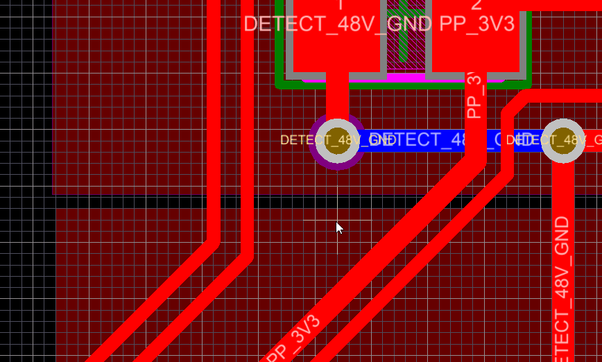
Altium Tip - Display of clearance boundaries during routing
Visualize design rule clearances in real-time during PCB routing
One thing that I find very helpful while routing is to display all clearance boundaries, this way you know how far you can go or squeeze all the traces as close as the rules allow it.
CTRL + W while routing and you are good to go!